


주메뉴
- About IBS 연구원소개
-
Research Centers
연구단소개
- Research Outcomes
- Mathematics
- Physics
- Center for Theoretical Physics of the Universe(Particle Theory and Cosmology Group)
- Center for Theoretical Physics of the Universe(Cosmology, Gravity and Astroparticle Physics Group)
- Center for Exotic Nuclear Studies
- Center for Artificial Low Dimensional Electronic Systems
- Center for Underground Physics
- Center for Axion and Precision Physics Research
- Center for Theoretical Physics of Complex Systems
- Center for Quantum Nanoscience
- Center for Van der Waals Quantum Solids
- Chemistry
- Life Sciences
- Earth Science
- Interdisciplinary
- Institutes
- Korea Virus Research Institute
- News Center 뉴스 센터
- Career 인재초빙
- Living in Korea IBS School-UST
- IBS School 윤리경영

주메뉴
- About IBS
-
Research Centers
- Research Outcomes
- Mathematics
- Physics
- Center for Theoretical Physics of the Universe(Particle Theory and Cosmology Group)
- Center for Theoretical Physics of the Universe(Cosmology, Gravity and Astroparticle Physics Group)
- Center for Exotic Nuclear Studies
- Center for Artificial Low Dimensional Electronic Systems
- Center for Underground Physics
- Center for Axion and Precision Physics Research
- Center for Theoretical Physics of Complex Systems
- Center for Quantum Nanoscience
- Center for Van der Waals Quantum Solids
- Chemistry
- Life Sciences
- Earth Science
- Interdisciplinary
- Institutes
- Korea Virus Research Institute
- News Center
- Career
- Living in Korea
- IBS School


News Center

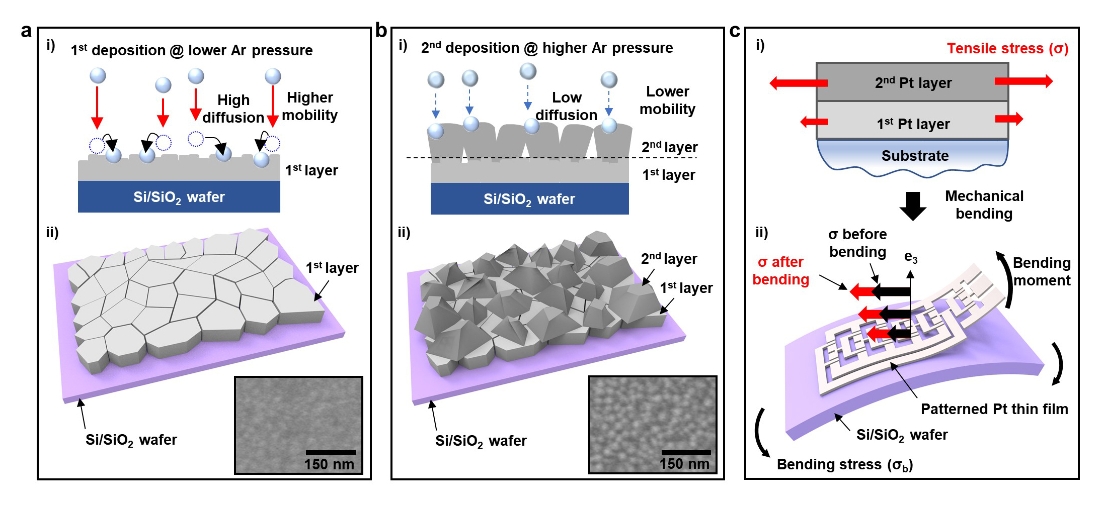
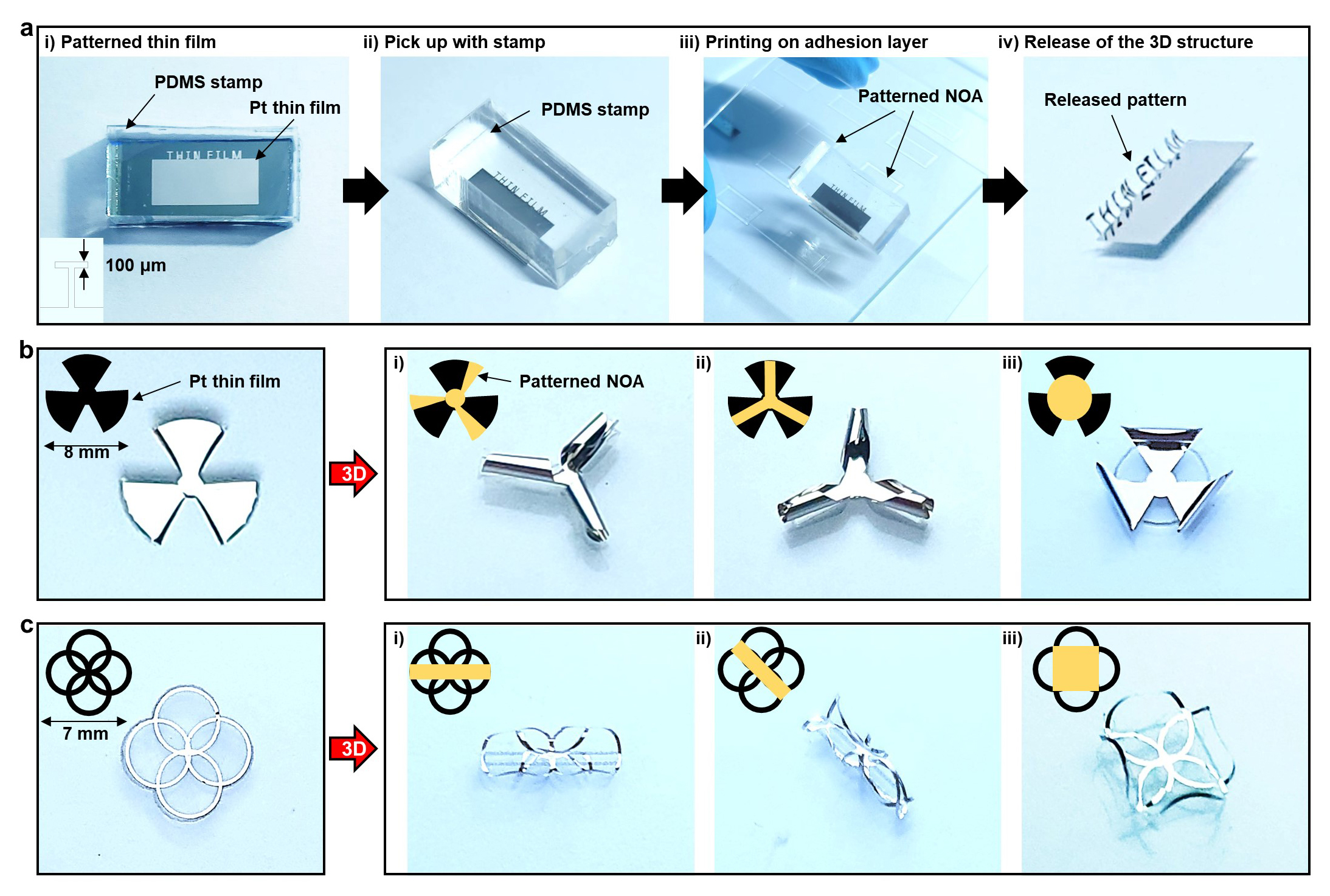
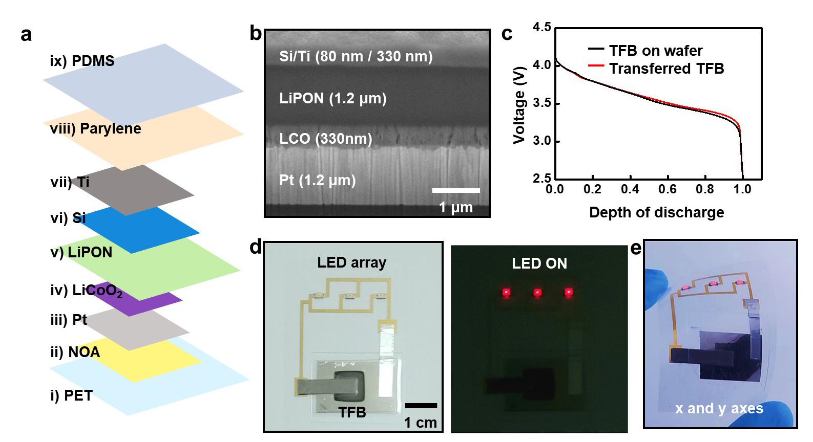
New Method for Transfer Printing of Flexible Electronics- A facile, versatile, and damage-free dry transfer printing strategy is developed based on stress control of the deposited thin films - Researchers at the Institute for Basic Science (IBS), South Korea, have developed an innovative dry transfer printing technique for flexible electronic devices. This method, spearheaded by Prof. KIM Dae-Hyeong, Dr. LEE Sangkyu, (IBS Center for Nanoparticle Research), and Prof. KIM Jihoon (Pusan University), allows for the transfer of high-quality electronic materials without damage, a significant advancement in the field. Typically, high-quality electronic materials are synthesized and processed at high temperatures to achieve the necessary crystalline structures and electrical properties. These high temperatures, however, make it challenging to process such materials directly on flexible or stretchable substrates. Hence for building flexible/stretchable devices, the electronics must be “transfer printed” from solid to soft substrate. Existing transfer printing technologies issues such as the use of toxic chemicals and potential mechanical damage during the transfer process. To address this issue, various methods such as laser or thermal processes and delamination in water have been developed. However, these methods require expensive equipment, involve additional post-processing, or are limited to specific environments. Additionally, it is challenging to use conventional transfer printing for high-quality electronic materials that require high-temperature treatment to form crystalline structures. To overcome these challenges, the research team developed a damage-free dry transfer printing method that controls stress within thin films. This new method allows metal and oxide thin films, processed at high temperatures, to be transferred to flexible substrates without damage. By adjusting sputtering parameters, the team controlled the type and magnitude of stress within the thin film. They created bilayer structures with varying stresses to maximize the stress gradient and applied additional tensile stress through external bending deformation. This process maximizes the strain energy release rate, allowing reliable delamination by surpassing the interfacial strength between the thin film and the substrate. "Our transfer method avoids toxic substances, minimizes device damage, and eliminates the need for post-processing, resulting in shorter transfer times," said Dr. SHIN Yoonsu, first co-author. "It can transfer large areas as well as micro-scale patterns, making it highly versatile." The team demonstrated that greater stress gradients within thin films result in larger bending moments, causing them to curl and transform from a two-dimensional (2D) thin film into a three-dimensional (3D) structure. The configuration of 3D structures can be adjusted by the pattern of the adhesive layer during transfer printing, allowing for the design and fabrication of desired structures to meet various requirements. Dr. LEE Sangkyu, one of the corresponding authors, emphasized, "The key to this research is the development of a damage-free dry transfer printing technique by controlling only material properties, unlike previous studies." He added, "We plan to further research the fabrication of diverse 3D devices, leveraging the technology to transform 2D thin films into 3D structures, beyond the simple 2D flexible battery devices demonstrated in the paper." "Transfer printing technology has applications across fields such as flexible electronics, optoelectronics, bioelectronics, and energy devices. Our method offers significant advantages for producing high-density 2D and 3D functional thin film structures without damage, greatly benefiting the development of new high-performance electronic devices," remarked Prof. KIM Dae-Hyeong.
Notes for editors
- References
- Media Contact
- About the Institute for Basic Science (IBS)
|
| Next | |
|---|---|
| before |
- Content Manager
- Public Relations Team : Yim Ji Yeob 042-878-8173
- Last Update 2023-11-28 14:20
55, Expo-ro, Yuseong-gu, Daejeon, Korea, 34126
Tel. +82-42-878-8114 | Fax. +82-42-878-8079 | E-mail. webmaster@ibs.re.kr
Copyright(c) IBS. All Rights Reserved.
