


주메뉴
- About IBS 연구원소개
-
Research Centers
연구단소개
- Research Outcomes
- Mathematics
- Physics
- Center for Theoretical Physics of the Universe(Particle Theory and Cosmology Group)
- Center for Theoretical Physics of the Universe(Cosmology, Gravity and Astroparticle Physics Group)
- Center for Exotic Nuclear Studies
- Center for Artificial Low Dimensional Electronic Systems
- Center for Underground Physics
- Center for Axion and Precision Physics Research
- Center for Theoretical Physics of Complex Systems
- Center for Quantum Nanoscience
- Center for Van der Waals Quantum Solids
- Chemistry
- Life Sciences
- Earth Science
- Interdisciplinary
- Institutes
- Korea Virus Research Institute
- News Center 뉴스 센터
- Career 인재초빙
- Living in Korea IBS School-UST
- IBS School 윤리경영

주메뉴
- About IBS
-
Research Centers
- Research Outcomes
- Mathematics
- Physics
- Center for Theoretical Physics of the Universe(Particle Theory and Cosmology Group)
- Center for Theoretical Physics of the Universe(Cosmology, Gravity and Astroparticle Physics Group)
- Center for Exotic Nuclear Studies
- Center for Artificial Low Dimensional Electronic Systems
- Center for Underground Physics
- Center for Axion and Precision Physics Research
- Center for Theoretical Physics of Complex Systems
- Center for Quantum Nanoscience
- Center for Van der Waals Quantum Solids
- Chemistry
- Life Sciences
- Earth Science
- Interdisciplinary
- Institutes
- Korea Virus Research Institute
- News Center
- Career
- Living in Korea
- IBS School


News Center

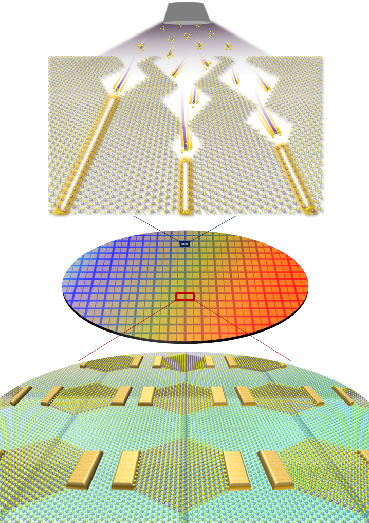
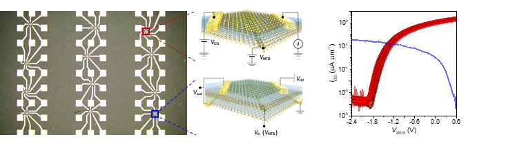
Scientists Discover Way to “Grow” Sub-Nanometer Sized Transistors- Opening the Path to Next-Generation Semiconductors through Epitaxial Growth of New Van der Waals Materials - A research team led by Director JO Moon-Ho of the Center for Van der Waals Quantum Solids within the Institute for Basic Science (IBS) has implemented a novel method to achieve epitaxial growth of 1D metallic materials with a width of less than 1 nm. The group applied this process to develop a new structure for 2D semiconductor logic circuits. Notably, they used the 1D metals as a gate electrode of the ultra-miniaturized transistor. Integrated devices based on two-dimensional (2D) semiconductors, which exhibit excellent properties even at the ultimate limit of material thickness down to the atomic scale, are a major focus of basic and applied research worldwide. However, realizing such ultra-miniaturized transistor devices that can control the electron movement within a few nanometers, let alone developing the manufacturing process for these integrated circuits, has been met with significant technical challenges. The degree of integration in semiconductor devices is determined by the width and control efficiency of the gate electrode, which controls the flow of electrons in the transistor. In conventional semiconductor fabrication processes, reducing the gate length below a few nanometers is impossible due to the limitations of lithography resolution. To solve this technical problem, the research team leveraged the fact that the mirror twin boundary (MTB) of molybdenum disulfide (MoS₂), a 2D semiconductor, is a 1D metal with a width of only 0.4 nm. They used this as a gate electrode to overcome the limitations of the lithography process. In this study, the 1D MTB metallic phase was achieved by controlling the crystal structure of the existing 2D semiconductor at the atomic level, transforming it into a 1D MTB. This represents a significant breakthrough not only for next-generation semiconductor technology but also for basic materials science, as it demonstrates the large-area synthesis of new material phases through artificial control of crystal structures. The International Roadmap for Devices and Systems (IRDS) by the IEEE predicts semiconductor node technology to reach around 0.5 nm by 2037, with transistor gate lengths of 12 nm. The research team demonstrated that the channel width modulated by the electric field applied from the 1D MTB gate can be as small as 3.9 nm, significantly exceeding the futuristic prediction. The 1D MTB-based transistor developed by the research team also offers advantages in circuit performance. Technologies like FinFET or Gate-All-Around, adopted for the miniaturization of silicon semiconductor devices, suffer from parasitic capacitance due to their complex device structures, leading to instability in highly integrated circuits. In contrast, the 1D MTB-based transistor can minimize parasitic capacitance due to its simple structure and extremely narrow gate width. Director JO Moon-Ho commented, "The 1D metallic phase achieved through epitaxial growth is a new material process that can be applied to ultra-miniaturized semiconductor processes. It is expected to become a key technology for developing various low-power, high-performance electronic devices in the future." This research was published on July 3rd in the journal Nature Nanotechnology.
Notes for editors
- References
- Media Contact
- About the Institute for Basic Science (IBS)
|
| Next | |
|---|---|
| before |
- Content Manager
- Public Relations Team : Yim Ji Yeob 042-878-8173
- Last Update 2023-11-28 14:20
55, Expo-ro, Yuseong-gu, Daejeon, Korea, 34126
Tel. +82-42-878-8114 | Fax. +82-42-878-8079 | E-mail. webmaster@ibs.re.kr
Copyright(c) IBS. All Rights Reserved.
