주메뉴
- About IBS 연구원소개
-
Research Centers
연구단소개
- Research Outcomes
- Mathematics
- Physics
- Center for Theoretical Physics of the Universe(Particle Theory and Cosmology Group)
- Center for Theoretical Physics of the Universe(Cosmology, Gravity and Astroparticle Physics Group)
- Center for Exotic Nuclear Studies
- Center for Artificial Low Dimensional Electronic Systems
- Center for Underground Physics
- Center for Axion and Precision Physics Research
- Center for Theoretical Physics of Complex Systems
- Center for Quantum Nanoscience
- Center for Van der Waals Quantum Solids
- Chemistry
- Life Sciences
- Earth Science
- Interdisciplinary
- Center for Neuroscience Imaging Research(Neuro Technology Group)
- Center for Neuroscience Imaging Research(Cognitive and Computational Neuroscience Group)
- Center for Algorithmic and Robotized Synthesis
- Center for Genome Engineering
- Center for Nanomedicine
- Center for Biomolecular and Cellular Structure
- Center for 2D Quantum Heterostructures
- Center for Quantum Conversion Research
- Institutes
- Korea Virus Research Institute
- News Center 뉴스 센터
- Career 인재초빙
- Living in Korea IBS School-UST
- IBS School 윤리경영


주메뉴
- About IBS
-
Research Centers
- Research Outcomes
- Mathematics
- Physics
- Center for Theoretical Physics of the Universe(Particle Theory and Cosmology Group)
- Center for Theoretical Physics of the Universe(Cosmology, Gravity and Astroparticle Physics Group)
- Center for Exotic Nuclear Studies
- Center for Artificial Low Dimensional Electronic Systems
- Center for Underground Physics
- Center for Axion and Precision Physics Research
- Center for Theoretical Physics of Complex Systems
- Center for Quantum Nanoscience
- Center for Van der Waals Quantum Solids
- Chemistry
- Life Sciences
- Earth Science
- Interdisciplinary
- Center for Neuroscience Imaging Research(Neuro Technology Group)
- Center for Neuroscience Imaging Research(Cognitive and Computational Neuroscience Group)
- Center for Algorithmic and Robotized Synthesis
- Center for Genome Engineering
- Center for Nanomedicine
- Center for Biomolecular and Cellular Structure
- Center for 2D Quantum Heterostructures
- Center for Quantum Conversion Research
- Institutes
- Korea Virus Research Institute
- News Center
- Career
- Living in Korea
- IBS School
News Center
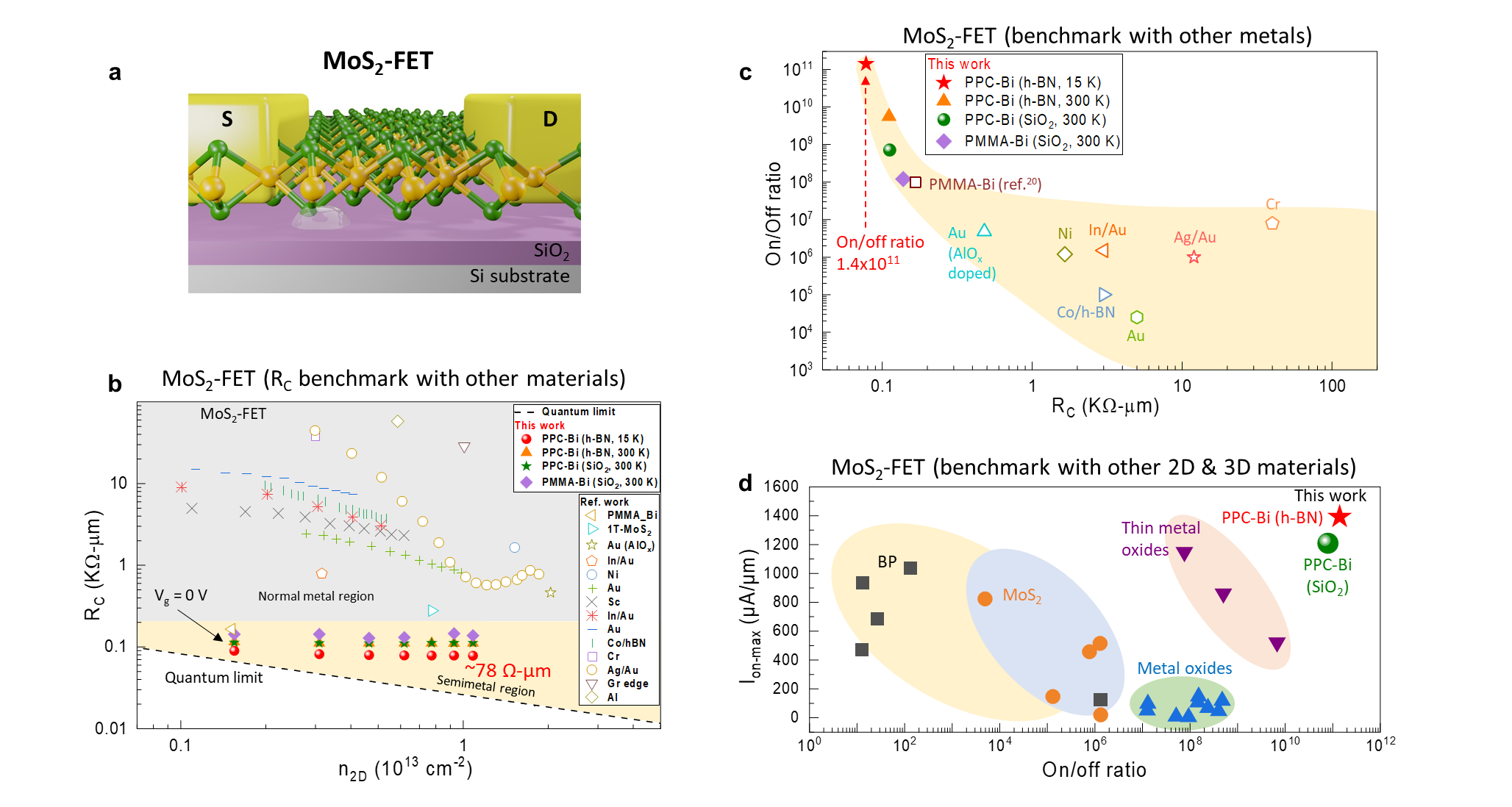
Pioneering beyond-silicon technology via residue-free field effect transistors- New transitional metal dichalcogenide field-effect transistors were found to have low ohmic contact resistance close to the quantum limit and record-high on/off ratio - A revolution in technology is on the horizon, and it’s poised to change the devices that we use. Under the distinguished leadership of Professor LEE Young Hee, a team of visionary researchers from the Center for Integrated Nanostructure Physics within the Institute for Basic Science (IBS), South Korea, has unveiled a new discovery that can greatly improve the fabrication of field-effect transistors (FET). A high-performance field-effect transistor (FET) is an essential building block for next-generation beyond-silicon-based semiconductor technologies. Current 3-dimensional silicon technology suffers from degradation of FET performances when the device is miniaturized past sub-3-nm scales. To overcome this limit, researchers have studied one-atom thick (~0.7 nm) two-dimensional (2D) transition metal dichalcogenides (TMDs) as an ideal FET platform over the last decade. Nevertheless, their practical applications are limited due to the inability to demonstrate integration at the wafer-scale. A major problem is the residues that occur during fabrication. Traditionally, polymethyl methacrylate (PMMA) is used as a supporting holder for device transfer. This material is notorious for leaving insulating residues on TMD surfaces, which often generates mechanical damage to the fragile TMD sheet during transfer. As an alternative to PMMA, several other polymers such as polydimethylsiloxane (PDMS), polyvinyl alcohol (PVA), polystyrene (PS), polycarbonate (PC), ethylene vinyl acetate (EVA), polyvinylpyrrolidone (PVP) and organic molecules including paraffin, cellulose acetate, naphthalene have all been proposed as a supporting holder. Nevertheless, residues and mechanical damages are inevitably introduced during transfer, which leads to degradation of FET performances. The IBS researchers addressed this problem and have made an intriguing breakthrough by successfully harnessing polypropylene carbonate (PPC) for residue-free wet transfer. Using PPC not only eliminated residue but also allowed for the production of wafer-scale TMD using chemical vapor deposition. Previous attempts at manufacturing large-scale TMDs often resulted in wrinkles, which occur during the transfer process. The weak binding affinity between the PPC and the TMD not only eliminated residues but wrinkles as well. Mr. Ashok MONDAL, the first author of the study said, “The PPC transfer method we chose enables us to fabricate centimeter-scale TMDs. Previously, TMD was limited to being produced using a stamping method, which generates flakes that are only 30-40 μm in size.” The researchers built a FET device using a semimetal Bi contact electrode with a monolayer of MoS2, which was transferred by the PPC method. Less than 0.08% of PPC residue was found to remain on the MoS2 layer. Thanks to the lack of interfacial residues, the device was found to have an ohmic contact resistance of RC ~78 Ω-µm, which is close to the quantum limit. An ultrahigh current on/off ratio of ~1011 at 15 K and a high on-current of ~1.4 mA/µm were also achieved using the h-BN substrate. This finding was the first in the world that demonstrated wafer-scale production and transfer of CVD-grown TMD. The state-of-the-art FET device produced in this way was found to have electrical properties that far exceed that of previously reported values. It is believed that this technology can be easily implemented using the currently available integrated circuit manufacturing technology. Dr. Chandan BISWAS, the co-corresponding author of the study said, “It is hoped that our success in the residue-free PPC transfer technique will encourage other researchers to develop further improvements in various TMD devices in the future.”
Notes for editors
- References
- Media Contact
- About the Institute for Basic Science (IBS)
|
| Next | |
|---|---|
| before |
- Content Manager
- Public Relations Team : Yim Ji Yeob 042-878-8173
- Last Update 2023-11-28 14:20


