주메뉴
- About IBS 연구원소개
-
Research Centers
연구단소개
- Research Outcomes
- Mathematics
- Physics
- Center for Theoretical Physics of the Universe(Particle Theory and Cosmology Group)
- Center for Theoretical Physics of the Universe(Cosmology, Gravity and Astroparticle Physics Group)
- Center for Exotic Nuclear Studies
- Center for Artificial Low Dimensional Electronic Systems
- Center for Underground Physics
- Center for Axion and Precision Physics Research
- Center for Theoretical Physics of Complex Systems
- Center for Quantum Nanoscience
- Center for Van der Waals Quantum Solids
- Chemistry
- Life Sciences
- Earth Science
- Interdisciplinary
- Center for Neuroscience Imaging Research(Neuro Technology Group)
- Center for Neuroscience Imaging Research(Cognitive and Computational Neuroscience Group)
- Center for Algorithmic and Robotized Synthesis
- Center for Genome Engineering
- Center for Nanomedicine
- Center for Biomolecular and Cellular Structure
- Center for 2D Quantum Heterostructures
- Center for Quantum Conversion Research
- Institutes
- Korea Virus Research Institute
- News Center 뉴스 센터
- Career 인재초빙
- Living in Korea IBS School-UST
- IBS School 윤리경영


주메뉴
- About IBS
-
Research Centers
- Research Outcomes
- Mathematics
- Physics
- Center for Theoretical Physics of the Universe(Particle Theory and Cosmology Group)
- Center for Theoretical Physics of the Universe(Cosmology, Gravity and Astroparticle Physics Group)
- Center for Exotic Nuclear Studies
- Center for Artificial Low Dimensional Electronic Systems
- Center for Underground Physics
- Center for Axion and Precision Physics Research
- Center for Theoretical Physics of Complex Systems
- Center for Quantum Nanoscience
- Center for Van der Waals Quantum Solids
- Chemistry
- Life Sciences
- Earth Science
- Interdisciplinary
- Center for Neuroscience Imaging Research(Neuro Technology Group)
- Center for Neuroscience Imaging Research(Cognitive and Computational Neuroscience Group)
- Center for Algorithmic and Robotized Synthesis
- Center for Genome Engineering
- Center for Nanomedicine
- Center for Biomolecular and Cellular Structure
- Center for 2D Quantum Heterostructures
- Center for Quantum Conversion Research
- Institutes
- Korea Virus Research Institute
- News Center
- Career
- Living in Korea
- IBS School
News Center
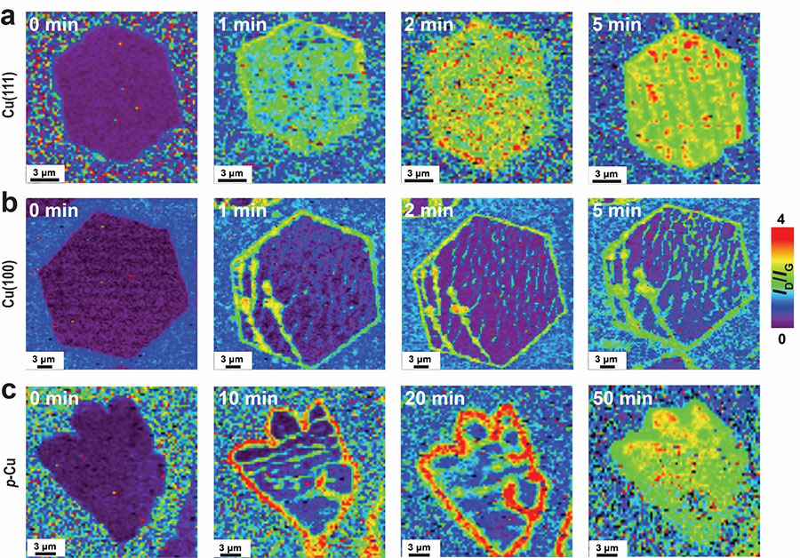
Compressive stress in single crystal graphene drives chemistry on the graphene surfaceResearchers synthesize a new 2D Metal Organic Framework with an ever-growing list of possible applications Chemical vapor deposition (CVD) growth of graphene on metal substrates, especially on copper (Cu) foils, is an effective and popular technique to synthesize graphene approaching perfect crystallinity. Covalent chemical functionalization of defect-free (and thus the most chemically inert) graphene on Cu with deliberately chosen appending groups is not only fundamentally important for understanding its chemistry, but also for tailoring its structures and properties, and could be beneficial in practical uses such as for electrochemical sensors, optical devices, non-corroding current collectors, and as electrodes in electrical energy storage systems, among other reasons. The chemical reactivity of graphene on Cu foil substrates is a currently a topic of fundamental scientific study.
To elucidate the reaction behaviors of graphene on Cu, the IBS research team led by Rodney S. Ruoff at the Center for Multidimensional Carbon Materials, who is also a Distinguished Professor at the Ulsan National Institute of Science and Technology (UNIST), along with Dr. Xu Zhang and coauthors, employed their newly-developed single-crystal graphenes on large-area Cu(111) and Cu(100) foils, as well as polycrystalline graphene grown on commercial polycrystalline Cu, to study some particular chemical reactions including a newly-developed reductive functionalization of graphene originally proposed by coauthor Prof. Christopher W. Bielawski. They found that the reaction occurs much more readily on single-crystal graphene on Cu(111) such that uniform functionalization of single-crystal graphene islands, and separately of completely grown continuous single-crystal graphene films, could be obtained. The extent of reaction is even higher than for graphene transferred onto silicon wafers having an oxide layer, a well-studied platform with relatively high reactivities. In contrast, graphene islands and continuous films grown on Cu(100) and polycrystalline Cu foils reacted to a much smaller extent. It was learned in the study that the size of the graphene islands on the Cu(111) has no influence on the functionalization, as further demonstrated by the similar efficiency of functionalization for continuous single-layer graphene films on Cu(111); this strongly implies that the reaction selectively takes place on the topside of graphene. Based on a series of Raman spectroscopy studies along with other experimental techniques and theoretical calculations, the noticeable strong difference of graphene’s reactivity on Cu substrates of different surface crystal orientations is because the graphene is under compressive strain that is significantly larger (its biaxial strain is about 0.3%) on Cu(111) owing to lattice-induced friction between the epitaxial graphene and Cu(111). Such a friction, previously presented by collaborator Prof. Feng Ding, leader of the IBS CMCM Theory Group, is much smaller for graphene on other surface-oriented Cu foils, in which compressive strain is largely released (it is less than < 0.1%) by local deadhesion (the friction is too small!) and thus “graphene wrinkles” are formed.
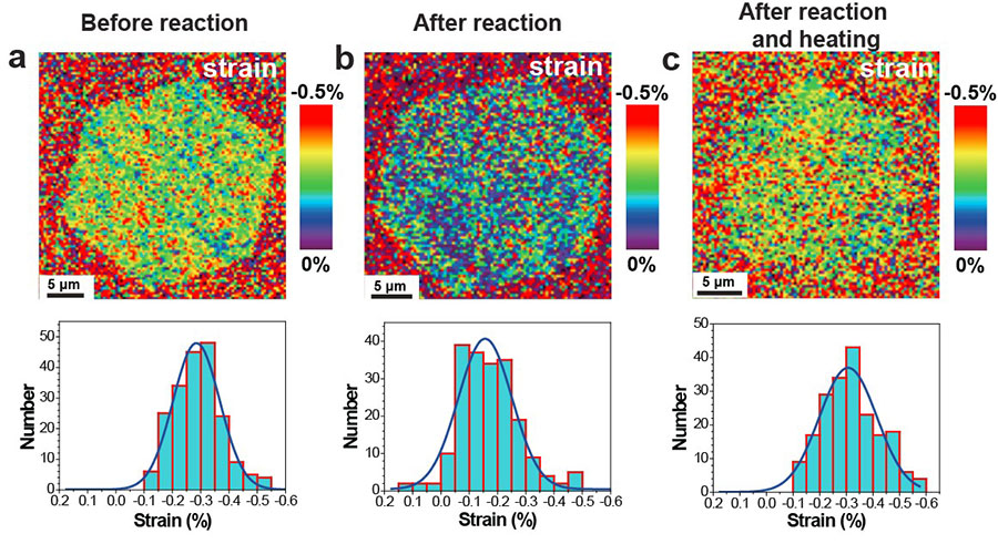
It was learned that the compressive strain present in the single-crystal graphene on the Cu(111) foil substrate could be changed by chemical reactions with the surface. Covalent functionalization was found to “relax” this compressive strain, and then when the functional groups were eliminated from the graphene by heating, the compressive strain was largely recovered. Since strain determines diverse physical properties of materials, this unique approach to “strain engineering” may be useful for particular types of graphene-based devices.
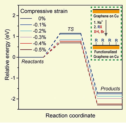
The influence of compressive strain on the energy barrier of graphene on Cu was investigated by theoretical calculations performed by Prof. Sang Kyu Kwak and his team members Mr. Dae Yeon Hwang and Mr. Sung O Park. The results showed that compressive strain was critical in lowering the energy barrier of the reactions. When the compressive strain was higher than 0.2%, the energy barrier for chemical reaction was reduced by around 0.3 eV. Study of the reaction kinetics of this chemical reaction on this single-crystal graphene on Cu(111) yielded a relatively low activation energy of around 20 kJ∙mol−1, a value favoring the spontaneous reaction at room temperature—a spontaneous reaction driven by release of this compressive strain. The scientists also investigated the covalent functionalization of bilayer graphene on Cu(111). The reactivity of bilayer graphene is influenced by the stacking mode of the two graphene layers. “Mis-oriented graphene” is more easily functionalized than graphene with no lattice rotation (“AB-stacked”). The team learned that the mis-oriented bilayer graphene also has a higher compressive strain than AB-stacked bilayer graphene, suggesting that the compressive strain may also influence the reactivity of bilayer graphene. Director Ruoff said, “For some applications, large-area single-crystal graphene, which can now be readily grown on our large-area Cu(111) foils, is likely superior to polycrystalline graphene grown on polycrystalline Cu foils. Our findings about the effect of Cu surface orientation on the covalent chemistry of graphene sheds light on the fundamental chemistry of single-crystal graphene and the role that compressive strain can play in some reactions, which could find many applications; one reason that this might be immediately useful, is that the continuous single-crystal graphene films are “automatically” under compressive strain when removed from the CVD growth chamber—and that compressive stress at the interface between the single crystal copper surface and the single crystal graphene—provides a chemical driving force for reacting the top surface—the exposed surface—of the graphene.” This research was supported by the Institute for Basic Science and has been published in the journal Chemistry of Materials: https://pubs.acs.org/doi/10.1021/acs.chemmater.9b01729 Notes for editors - References - Media Contact - About the Institute for Basic Science (IBS) |
|||
|
|
| Next | |
|---|---|
| before |
- Content Manager
- Public Relations Team : Yim Ji Yeob 042-878-8173
- Last Update 2023-11-28 14:20


